
TRIPS Prototype System
The TRIPS project team is building a full system prototype to demonstrate the feasibility of this new technology. The prototype hardware consists of custom TRIPS chips mounted on custom TRIPS circuit boards. Each TRIPS chip contains two advanced processor cores that support the TRIPS EDGE architecture and 1 megabyte of on-chip memory. A TRIPS motherboard includes 4 TRIPS chips and 8 gigabytes of DRAM (2 gigabytes per chip). The entire TRIPS system is scalable to 32 TRIPS chips and 64 gigabytes. At the prototype target clock frequency of 500 MHz, the peak performance is 500 gigaflops.
TRIPS Prototype Chip
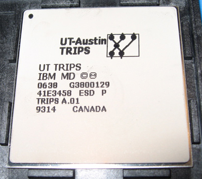
The TRIPS prototype chip is a 170 million transistor custom ASIC designed in a 130nm technology. The UT-Austin TRIPS team partnered with IBM microelectronics for ASIC physical design, including placement, routing, and fabrication.
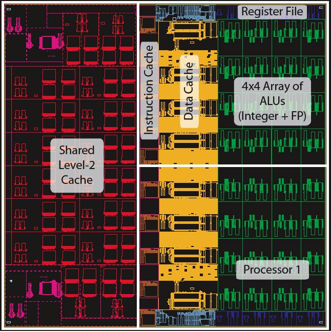
Each of the two processor cores can execute up to 16 out-of-order operations (integer or floating point) per cycle, from a window of up to 1,024 in-flight instructions. The processor core is composed of multiple copies of five different types of tiles interconnected via microarchitectural networks. Each core may be configured in a single threaded mode or in a 4-thread multithreaded mode in which instructions from multiple threads may execute simultaneously. A TRIPS processor core is fundamentally distributed for technology scalability and to provide high bandwidth to the instruction cache, data cache, and register file through partitioning and replication.
The chip also contains a 1MB level-two static non-uniform cache access (NUCA) memory system to keep the processor cores fed at high data bandwidth. The NUCA system is composed of 16 64KB memory tiles interconnected via an on-chip network fabric. Individual memory tiles may be configured as a part of the cache or as a part of physically mapped memory. The memory netork also includes two direct memory access (DMA) controllers, two DDR DRAM controllers, and a network controller to connect gluelessly to adjacent TRIPS chips.
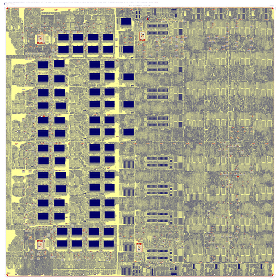
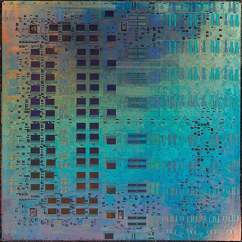
The diagrams below show a fabricated chip in a 47mm square package, a floorplan of the TRIPS chip colorcoded to highlight the distinct tiles, and a detailed chip plot. Click on each diagram to see a larger version.
 |
 |
 |
 |
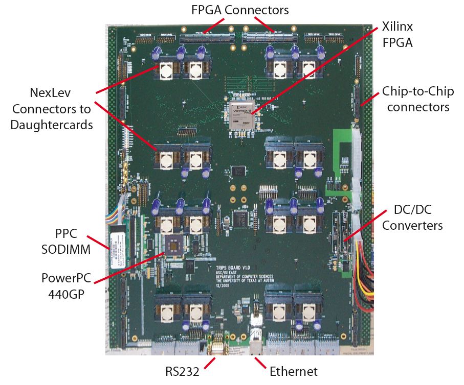
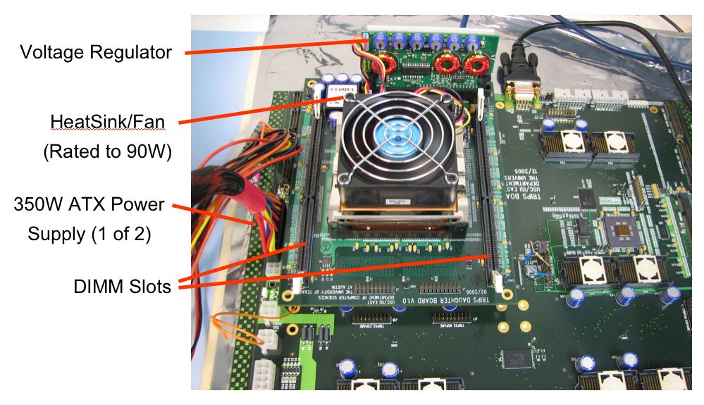
TRIPS Circuit Boards
A TRIPS chip is mounted on a daughtercard along with two 1-gigabyte DRAM DIMMs, voltage converters, and power regulators. Four daughtercards are attached to the TRIPS motherboard using high-density NexLev connectors. The motherboard also contains an embedded PowerPC 440GP chip, 2 low-profile SODIMMs, an Xilinx FPGA chip, and numerous connectors. Both daughtercard and motherboard were designed by TRIPS partners at USC-ISI.
The TRIPS system is controlled by a runtime monitor executing on a host PC. The monitor sends read and write commands to the on-board PowerPC via ethernet, which relays them to a selected TRIPS chip. With this mechanism, the monitor may read or write any memory location or register on any TRIPS chip. TRIPS can request that the monitor load a program, run a program, read the contents of memory, as well as many other tasks to evaluate software on the TRIPS system.
TRIPS chips communicate directly though the chip-to-chip network. This mesh network connects Manhattan nearest neighbor chips on a board. Chip-to-chip network links are exported to connectors on the edge of the motherboard. High speed cables bridge between adjacent boards.
Click on the photographs of the annotated TRIPS motherboard and daughtercard below to see larger images.
 |
 |